

30V/350mA High Brightness LED Constant Current Driver PT4211
PT4211 Description
PT4211 is a step-down constant current source operating in continuous inductor current conduction mode, specifically designed to drive 1 to 3 series-connected LEDs. It accepts an input voltage range from 5V to 30V, with adjustable output current up to 350mA. PT4211 integrates a power switch and adopts high-side current sensing. The average LED current is set via an external resistor. A dedicated DIM pin accepts a wide range of PWM dimming signals. When the DIM voltage is below 0.4V, the power switch turns off and PT4211 enters standby mode with ultra-low operating current.
PT4211 is available in SOT23-5 package.
PT4211 Features
● Minimal external components
● Wide input voltage range: 5V to 30V
● Up to 350mA output current
● Dedicated DIM pin supports PWM dimming
● Output current accuracy of ±3%
● Built-in LED open-circuit protection
● Efficiency up to 93%
● Adjustable constant current control
● Soft thermal shutdown minimizes LED flickering at high temperatures
● SOT23-5 package
PT4211 Applications
● MR16 lighting systems
● Automotive LED lighting
● LED emergency lamps
● LED indicator lights
PT4211Ordering Information
Package
| Temperature Range
| Ordering Model
| Packing
| Marking
|
SOT23-5
| -40℃ to 85℃ | PT4211E23E
| Tape and Reel 3000 units | 4211 xxxxxX |
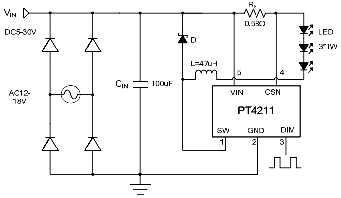
PT4211 Typical Application Circuit

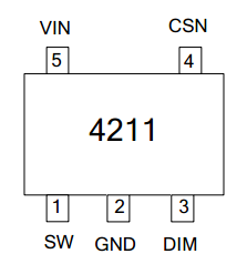
PT4211 Pin Configuration

PT4211 Operating Principle
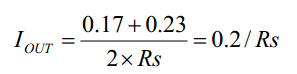
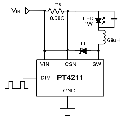
PT4211 forms a self-oscillating, continuous inductor current mode step-down constant current LED controller together with inductor (L) and current sense resistor (RS). At power-up of VIN, the initial current in inductor (L) and sense resistor (RS) is zero, and the LED output current is also zero. The output of the CS comparator is high, turning on the internal power switch and pulling SW low. Current flows from VIN to GND through L, RS, LED string and the internal power switch. The rising slope of the current is determined by VIN, inductance and LED forward voltage, generating a voltage VCSN across RS. When (VIN-VCSN) > 230mV, the CS comparator output goes low, turning off the power switch. Current then circulates through L, RS, LED and Schottky diode (D) with a falling slope. When (VIN-VCSN) < 170mV, the power switch turns on again. As a result, the average LED current is

The high-side current sensing architecture minimizes external components. With a 1% tolerance sense resistor, LED output current accuracy is within ±3%.
PT4211 supports PWM dimming via the DIM pin. LED current is disabled when DIM voltage is below 0.4V and enabled when above 1.7V. The PWM dimming frequency ranges from 100Hz to over 20kHz, with the maximum dimming frequency dependent on the operating frequency.
The DIM pin can be left floating in normal operation; an internal 300kΩ resistor pulls it up to 5V. When DIM voltage is below 0.4V, the internal power switch turns off and LED current drops to zero. During shutdown, the internal regulator remains in standby with a quiescent current of 95µA.
In addition, internal soft thermal protection reduces LED flickering during overtemperature conditions and enhances reliability. If die temperature exceeds 135°C due to abnormal load current, PT4211 automatically reduces LED current to prevent further temperature rise. If temperature rises above 150°C, thermal shutdown (TSD) turns off the device until temperature drops by 15°C.
PT4211 Application Information
Setting LED Average Current via External Sense Resistor RS
The average LED current is determined by resistor RS connected between VIN and CSN:
IOUT=0.2/Rs
This equation applies when DIM is floating or biased above 1.7V (but below 5V). With maximum current set, output current can be adjusted by applying PWM pulses with varying duty cycles to the DIM pin.
Dimming with PWM Signal
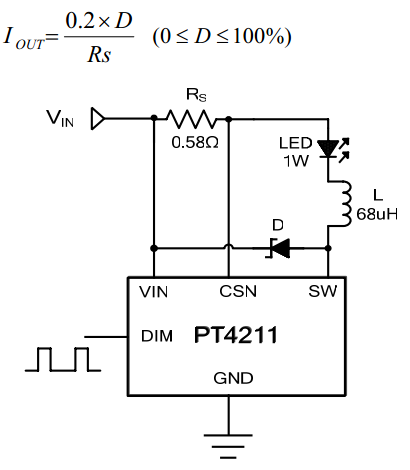
The maximum average LED current is set by RS between VIN and CSN. Dimming is achieved by reducing the average current using PWM signals with variable duty cycles on the DIM pin, as calculated below:

With PWM dimming, LED output current can be adjusted from 0% to 100%. Brightness is determined by the duty cycle of the PWM signal. For example, a 25% duty cycle results in 25% of the nominal current (0.2/RS). PWM dimming preserves LED color consistency better than analog dimming. The maximum PWM dimming frequency is limited by the system operating frequency. Lower dimming frequencies improve linearity, while frequencies above 100Hz are recommended to avoid visible flicker.
Shutdown Mode
The system enters shutdown by applying a voltage below 0.4V to DIM, with typical quiescent current below 95μA.
LED Open-Circuit Condition
PT4211 features inherent open-circuit protection. If the load opens, the SW pin floats and the device enters a safe low-power mode, protecting both LEDs and the IC. Normal operation resumes once the load is reconnected.
Bypass Capacitor
A low-ESR bypass capacitor must be placed close to the input supply. Higher ESR degrades efficiency. The capacitor should handle high peak currents and average input current to reduce supply disturbance. For DC input, a minimum of 4.7µF is recommended; for AC or low-voltage input, a 100µF tantalum or equivalent capacitor is suggested. The capacitor should be placed as close to the IC input pins as possible. X5R/X7R dielectric capacitors are recommended for stability over temperature and voltage.
Inductor Selection
Recommended inductor value for PT4211 is 47µH ~ 100µH. The inductor’s saturation current should be 30% to 50% higher than the maximum output current. Larger inductance is preferred at higher input voltages to improve current regulation and reliability. The inductor should be placed close to VIN and SW pins to minimize parasitic resistance and efficiency loss.
Recommended inductor selection is shown below:

For example, the following CoilCraft inductors are suitable:

Inductor selection must also comply with the maximum operating frequency specification of PT4211.
Diode Selection
To ensure high efficiency and performance, diode (D) should be a Schottky barrier diode with fast recovery, low forward voltage drop, low parasitic capacitance and low leakage. Current and voltage ratings should be sized for the application with at least 30% margin
for reliable operation. Attention should be paid to Schottky reverse leakage at temperatures above 85°C, as excessive leakage increases power dissipation. For AC12V rectification, a low-VF Schottky diode is mandatory to minimize losses.
Output Ripple Reduction
A highly effective method to reduce output current ripple is to place a capacitor in parallel with the LED string as shown:

A 1µF capacitor typically reduces ripple by about one-third. Larger output capacitors further suppress ripple. Note that the output capacitor does not affect operating frequency or efficiency but increases startup delay and constrains dimming frequency.
Operation at Low Input Voltage
When input voltage is close to output voltage, the system operates at high duty cycles, especially below 10V input, increasing power dissipation. Prolonged operation may trigger
thermal protection, resulting in lower output current than set value. A reasonable voltage differential between input and output is recommended for stable operation. Low input voltage generally reduces overall efficiency.
Thermal Considerations
Avoid exceeding power limits in high ambient temperature or high-power load conditions. Efficiency is typically lowest at minimum input voltage, which may cause temperature rise. Unsuitable inductors or excessive parasitic capacitance at switching nodes also reduce efficiency.
Thermal Shutdown (TSD)
PT4211 integrates thermal shutdown protection (TSD) for reliable operation. When die temperature exceeds 135°C, the device enters thermal pre-regulation and reduces load current. If temperature continues to rise to 150°C, the IC shuts down completely. It resumes operation only after temperature drops below 140°C.
PCB Layout Guidelines
Proper PCB layout is critical for system stability and low noise. Multi-layer PCBs effectively suppress noise coupling. Input bypass capacitors should be connected to a separate ground path to minimize noise in the current loop.
SW Node
The SW pin is a high-speed switching node; PCB traces should be kept as short as possible. The IC GND pin must have a solid ground connection.
Inductor and Current Sense Resistor
The inductor should be placed close to the corresponding pins to avoid efficiency degradation. Minimize parasitic resistance across RS to ensure accurate current sensing.