DW8533 Non-Isolated Buck LED Regulator With PFC and High Voltage MOSFET
DONGWOON-DW8533 Order information
ORDERING PART NUMBER
| MARKING
| PACKAGE
| TRANSPORT MEDIA |
DW8533
| DW8533
xxxxxX
| SOP7
| 2500/Tape and Reel
|
DW8533 Non-Isolated Buck LED Regulator With PFC and High Voltage MOSFET General Description:
The DW8533 is a constant current LED regulator with high current accuracy which applies to single stage step-down power factor corrected LED drivers. 600V power MOS is integrated, which can significantly simplify the design of LED lighting system.
High accuracy of output current is achieved by sampling the output current directly. Critical conduction mode operation reduces the switching losses and largely increases the efficiency. DW8533 is supplied from the output directly, and auxiliary winding is not needed.
DW8533 has multi-protection functions which largely enhance the safety and reliability of the system, including VCC over-voltage protection, VCC UVLO, short-circuit protection, LED open protection, cycle-by-cycle current limit and over-temperature protection.
Non-Isolated Buck LED Regulator With PFC and High Voltage MOSFET DW8533 Features:
●No auxiliary winding;
●600V High voltage MOSFET integrated;
●High Current accuracy of line and load regulation ;
●High power factor with low output current-ripple;
●Critical conduction mode ;
●High efficiency over wide operating range;
●Cycle by Cycle current limit;
●LED short protection ;
●LED open protection ;
●Over-temperature protection;
●Compact SOP7 Package;
Non-Isolated Buck LED Regulator With PFC and High Voltage MOSFET DW8533 Applications:
●AC/DC LED driver applications
●Signage and decorative LED lighting
●General lighting of flat panel displays
●RGB backlight
●General purpose constant current source
●IBulb light
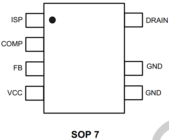
Non-Isolated Buck LED Regulator With PFC and High Voltage MOSFET DW8533 Pin Information

PIN No.(DW8533)
| DW8533 Pin Name | DW8533 Description |
1
| ISP | Output Current Sense Pin. The pin is used for output current control |
| 2 | COMP |
Compensation Pin for Internal Error Amplifier. Connect a capacitor between the pin and GND to compensate the internal feedback loop. |
| 3 | FB
|
Voltage Loop Feedback Pin. FB is used to detect LED open by sampling the output voltage |
| 4 | VCC
|
Power Supply Pin. This pin supplies current to the internal start-up circuit. This pin must be bypassed with a capacitor nearby. |
| 5 | GND
| Ground |
6
| GND
| Ground
|
| 7 | DARIN | DARIN of the MOSFET. |
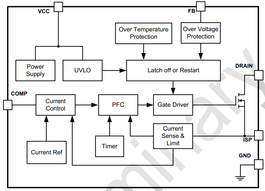
DW8533 Block Diagram:

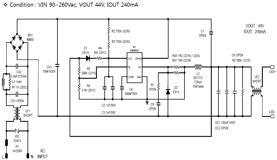
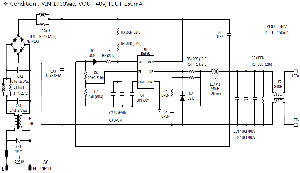
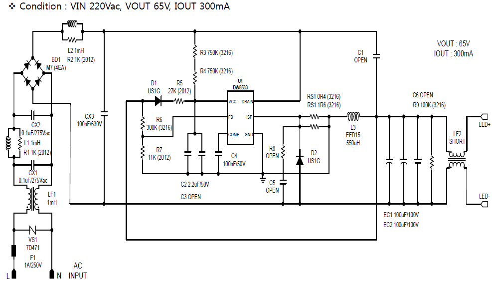
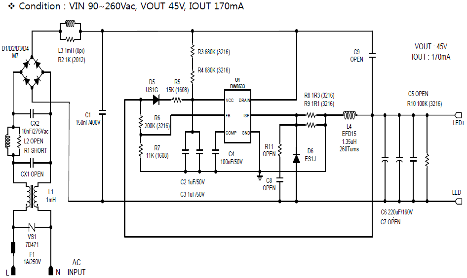
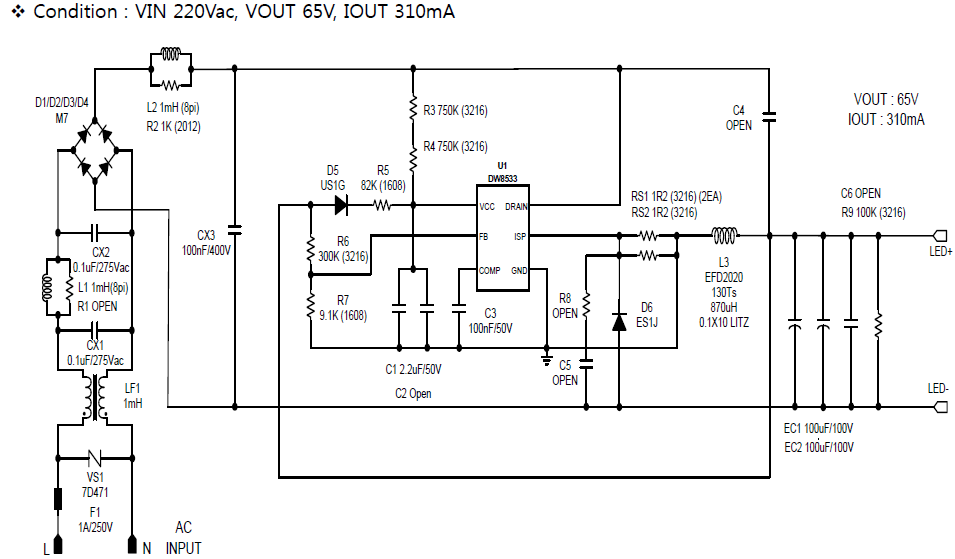
DW8533 Typical Application Circuit:

Absolute Maximum Ratings(1)
Symbol
| Parameter
| Ratings
|
VCC
| VCC Voltage
| 43V
|
GATE
| GATE Voltage
| 18V
|
ISP, COMP, FB
| ISP, COMP, FB Voltage
| -0.3V ~ 4.5V
|
θJA
| Package Thermal Resistance(2) | 96 ℃/W
|
θJC | Package Thermal Resistance(2) | 45 ℃/W
|
TSTG
| Storage Temperature
| -65 ~ 150 ℃
|
TJ | Junction temperature(3),(4) | 150℃
|
Note 1. Exceeding these ratings may damage the device.
2. Measured on JESD51-7, 4-layer PCB.
3. The DW8533 guarantees robust performance from -40°C to 150°C junction temperature. The junction temperature range specification is assured by design, characterization and correlation with statistical process controls.
4. The DW8533 includes thermal protection that is intended to protect the device in overload conditions. Thermal protection is active when junction temperature exceeds the maximum operating junction temperature. Continuous operation over the specified absolute maximum operating junction temperature may damage the device.
Absolute Maximum Ratings
Use of the IC in excess of absolute maximum ratings such as the applied voltage or operating temperature range (TJ) may result in IC damage. Assumptions should not be made regarding the state of the IC (short mode or open mode) when such damage is suffered. The implementation of a physical safety measure such as a fuse should be considered when use of the IC in a special mode when the absolute maximum ratings may be exceeded is anticipated.
DW8533 Recommended Operating Condition
Symbol
| Parameter
| Min.
| Typ.
| Max.
| Unit
|
VCC
| Supply voltage
| 20
|
| 30 | V |
FB
| FB voltage
| 1.6
|
| 2.6 | V |
TJ
| Junction Temperature
|
|
| 125 | ℃
|
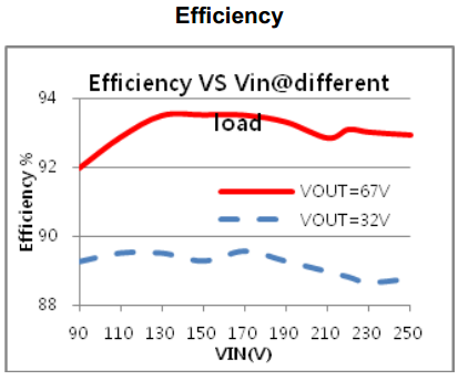
DW8533 Typical Operating Characteristics
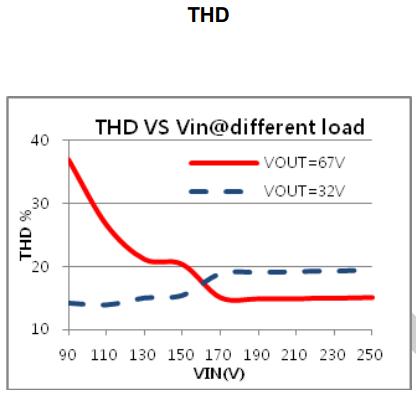
(VIN=85VAC~264VAC, VOUT=67V, Io=320mA, ,unless otherwise noted)


DW8533 Detailed Descriptions
The DW8533 is a constant current LED regulator which applies to non-isolation step-down LED system with power factor correction. 600V power MOS is integrated, which can significantly simplify the design of LED lighting system. DW8533 can achieve excellent line and load regulation, high efficiency and low BOM cost.
Start Up
When the pull-up resistor charges VCC up to 21V, the gate drive signal begins to switch, and the output begins to provide power to the VCC pin when the output is enough. An internal voltage clamp is attached to the VIN pin to prevent VCC from being too high. An internal 10mA current pulls the VCC down and stop switching when it is above 43V and restart switching when VCC is pulled down to 35V. When VCC is lower than 7.7V, it stops switching.
Loop Compensation
An integrator configuration is applied to the output current feedback loop with a capacitor connected to the COMP pin. For offline applications, the crossover frequency should be set much less than the line frequency of 120Hz or 100Hz. To have a good PFC performance, a capacitor of 0.1μF connected to COMP pin is recommended.
LED Over Temperature Protection
When DW8533 is hotter than 150°C, the chip stops switching, thus the output current decreases to zero; when the temperature is decreased to 135°C, the chip starts switching again.
LED Open Protection
The output voltage can be detected by the FB pin. When the FB voltage is higher than 3.0V, the LED open protection is triggered and the power MOSFET gate driver stops switching. After several seconds, the gate driver starts switching again.
The recommended FB pin voltage is about 2.5V at rated output,and it’s pull-up resistor is typically in hundreds KΩ level.
LED Short Protection
DW8533 judges LED short from the FB voltage. During a shorted LED condition, DW8533 reduces the internal command current to a very low level and slows down the switching frequency to 1.25 kHz to decrease the output current.
If LED short or LED open protection are false triggered by unreasonable PCB layout, a 20pF capacitor paralleled to FB pin and GND can solve the problem.
PCB Layout Guidelines
1. DW8533 The VCC pin must be locally bypassed with a capacitor.
2. Make the area of the power loop as small as possible in order to reduce the EMI radiation.
3. The chip should be far away from the heating components, such as MOSFET, transformer and diode.
4. Note the chip ground is not connected to the cathode of the input capacitor as usual.
Application Reference
VIN: 90VAC~264VAC
VOUT: 32~65V
IOUT: 320mA
PF: >0.9

Key words of this article:DW8533, Non-Isolated, Buck LED Regulator ,High PFC, High Voltage MOSFET


