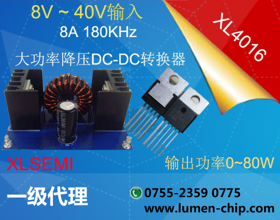
XL4016 is 8A 180KHz 40V Buck DC to DC Converter
8A 180KHz 40V Buck DC to DC Converter IC---XL4016 Buck CV 0~80W |
Product model
| Input Voltage
| Output Voltage | Max. switching current | Switching frequency
| Constant current setting
| Package
| Application note
| Datasheet
|
XL4016
| 8V~40V
| 1.25V~36V
| 8A
| 180KHz
| Adj (1.25V) | TO220-5L
|  | |
XL4016 General Description
The XL4016 is a 180 KHz fixed frequency PWM buck (step-down) DC/DC converter, capable of driving a 8A load with high efficiency, low ripple and excellent line and load regulation. Requiring a minimum number of external components, the regulator is simple to use and include internal frequency compensation and a fixed-frequency oscillator.
The PWM control circuit is able to adjust the duty ratio linearly from 0 to 100%. An over current protection function is built inside. When short protection function happens, the operation frequency will be reduced from 180KHz to 48KHz. An internal compensation block is built in to minimize external component count.
XL4016 Features
● Wide 8V to 40V Input Voltage Range
● Output Adjustable from 1.25V to 36V
● Maximum Duty Cycle 100%
● Minimum Drop Out 0.3V
● Fixed 180KHz Switching Frequency
● 8A Constant Output Current Capability
● Internal Optimize Power MOSFET
● High efficiency up to 96%
● IExcellent line and load regulation
● Built in thermal shutdown function
● Built in current limit function
● Built in output short protection function
● Built in input over voltage protection
● Available in TO220-5L package
XL4016 Applications
● LCD Monitor and LCD TV
● Portable instrument power supply
● Telecom / Networking Equipment
XL4016 Pin Configurations

XL4016 Pin Description
Pin Number
| Pin Name
| Description
|
| 1 | GND
| Ground Pin. Care must be taken in layout. This pin should be placed outside of the Schottky Diode to output capacitor ground path to prevent switching current spikes from inducing voltage noise into XL4016. |
| 2 | FB
| Feedback Pin (FB). Through an external resistor divider network, FB senses the output voltage and regulates it. The feedback threshold voltage is 1.25V. |
| 3 | SW
| Power Switch Output Pin (SW). SW is the switch node that supplies power to the output. |
| 4 | VC
| Internal Voltage Regulator Bypass Capacity. In typical system application, The VC pin connect a 1uf capacity to VIN. |
| 5 | VIN
| Supply Voltage Input Pin. XL4016 operates from a 8V to 40V DC voltage. Bypass Vin to GND with a suitably large capacitor to eliminate noise on the input. |
XL4016 Typical Application Circuit

XL4016 Typical Application Circuit (VIN=8V~40V, VOUT=5V/8A)
Function Block Diagram of XL4016

XL4016 Ordering Information
Order Information
| Marking ID
| Package Type
| Packing Type Supplied As
|
XL4016E1
| XL4016E1
| TO220-5L
| Tube
|
XLSEMI Pb-free products, as designated with “E1” suffix in the par number, are RoHS compliant.
Absolute Maximum Ratings(Note1)
Parameter
| Symbol
| Value
| Unit
|
Input Voltage
| Vin
| -0.3 to 45
| V
|
Feedback Pin Voltage
| VFB
| -0.3 to Vin
| V
|
Output Switch Pin Voltage
| VOutput
| -0.3 to Vin
| V
|
Power Dissipation
| PD
| Internally limited
| mW
|
Thermal Resistance (TO220-5L) (Junction to Ambient, No Heatsink, Free Air) | RJA
| 30
| ºC/W
|
Operating Junction Temperature
| TJ | -40 to 125
| ºC
|
Storage Temperature
| TSTG
| -65 to 150
| ºC
|
Lead Temperature (Soldering, 10 sec)
| TLEAD | 260
| ºC
|
ESD (HBM)
|
| >2000
| V
|
Note1: Stresses greater than those listed under Maximum Ratings may cause permanent damage to the device. This is a stress rating only and functional operation of the device at these or any other conditions above those indicated in the operation is not implied. Exposure to absolute maximum rating conditions for extended periods may affect reliability.
XL4016 Typical System Application (VOUT=5V/8A)
")
XL4016 System Parameters Test Circuit (VIN=8V~40V, VOUT=5V/8A)
Efficiency VS Load current

XL4016 System Efficiency Curve
XL4016 Typical System Application (VOUT=12V/6A)
")
XL4016 System Parameters Test Circuit (VIN=15V~40V, VOUT=12V/6A)

XL4016 System Efficiency Curve
XL4016 Typical System Application (TTL shutdown function)
Logic level signals shutdown function can be used in typical system application with external components. When the TTL high voltage above 3.3V(referenced to ground, lower than VIN), the converter will shutdown, input current less than 5mA; when the TTL Low voltage below 0.8V(referenced to ground), the converter will turn on.

XL4016 Schottky Diode Selection Table

Keywords: XL4016 XLSEMI