HIGH EFFICIENCY LOW EMI 30V 1.3A AUTOMOTIVE GRADE BUCK LED DRIVER AL8807Q
AL8807Q Ordering Information

Part Number
| Package Code
| Packaging (Note 9) | Packing: 13” Tape and Reel
| Qualification Grade (Note 10) |
AL8807QMP-13
| MP
| MSOP-8EP
| Quantity
| Tape Width
| Part Number Suffix
|
| 2500 | 12mm
| -13 | Automotive Grade
|
Note: 1. Pad layout as shown on Diodes Inc. suggested pad layout document AP02001, which can be found on our website at
http://www.diodes.com/datasheets/ap02001.pdf
2. AL8807Q has been qualified to AEC-Q100 grade 1 and is classi fied as “Automotive Grade” which supports PPAP documentation.
See AL8807 datasheet for commercial qualified versions.
AL8807Q Description
The AL8807Q is a step-down DC/DC converter designed to drive LEDs with a constant current. T he device can drive up to 9 LEDs,depending on the forward voltage of the LEDs, in series from a voltage source of 6V to 30V. Series connection of the LEDs provides identical LED currents resulting in uniform brightness and eliminating the need for ballast resistors. The AL8807Q switches at frequency up to 1MHz with controlled rise and fall times to reduce EMI. This allows the use of small size external components, hence minimizing the PCB area needed.
Maximum output current of AL8807Q is set via an external resistor connected between the VIN and SET input pins. Dimming is achieved
by applying either a DC voltage or a PWM signal at the CTRL input pin. An input voltage of 0.4V or lower at CTRL switches off the output MOSFET simplifying PWM dimming.
The AL8807Q has been qualified to AEC-Q100 Grade 1 and is Automotive Grade supporting PPAPs
AL8807Q Features
●LED driving current up to 1.3A
●Better than 5% accuracy
●High efficiency up to 96%
●Optimally controlled switching speeds
●Operating input voltage from 6V to 30V
●PWM/DC input for dimming control
●Built-in output open-circuit protection
●Automotive Grade with AEC-Q100 Qualification
●MSOP-8EP: Available in “Green” Molding Compound (No Br, Sb)
●Totally Lead-Free & Fully RoHS Compliant (Notes 1 & 2)
●Halogen and Antimony Free. “Green” Device (Note 3)
●Automotive Grade
●Qualified to AEC-Q100 Standards for High Reliability
●PPAP Capable (Note 4)
Notes: 1. No purposely added lead. Fully EU Directive 2002/95/EC (RoHS) & 2011/65/EU (RoHS 2) compliant.
2. See http://www.diodes.com/quality/lead_free.html for more information about Diodes Incorporated’s definitions of Halogen- a nd Antimony-free, "Green"
and Lead-free.
3. Halogen- and Antimony-free "Green” products are defined as those which contain <900ppm bromine, <900ppm chlorine (<1500ppm total Br + Cl) and
<1000ppm antimony compounds.
4. Automotive products are AEC-Q100 qualified and are PPAP capable. Automotive, AEC-Q100 and standard products are electricall y and thermally the same, except where specified. For more information, please refer to http://www.diodes.com/quality /product_compliance_definitions/.
AL8807Q Applications
●Automotive Interior LED Lamps
●Automotive Exterior LED Lamps
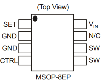
AL8807Q Pin Assignments

AL8807Q Pin Descriptions
Pin Name
| Pin Number
| Functions
|
SET
| 1 | Set Nominal Output Current Pin. Configure the output current of the device.
|
GND
| 2,3 | GND Pin
|
CTRL
| 4 | Dimming and On/Off Control Input.
●Leave floating for normal operation.
(VCTRL = VREF = 2.5V giving nominal average output current IOUTnom = 0.1/RS) ●Drive to voltage below 0.4V to turn off output current ●Drive with DC voltage (0.5V < VCTRL < 2.5V) to adjust output current from 20% to 100% of IOUTnom ●A PWM signal (low level ≤ 0.4V and high level > 2.6; transition times less than 1us) allows the output current to be adjusted below the level set by the resistor connected to SET input pin. |
SW
| 5,6 | Switch Pin. Connect inductor/freewheeling diode here, minimizing track length at this pin to reduce EMI.
|
N/C
| 7 | no connection
|
VIN
| 8
| Input Supply Pin. Must be locally decoupled to GND with > 2.2µF X7R ceramic capacitor – see applications section for more information. |
EP
| EP | Exposed pad/TAB connect to GND and thermal mass for enhanced thermal impedance. Should not be used as electrical ground conduction path. |
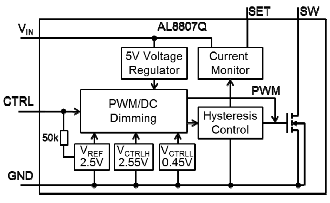
AL8807Q Functional Block Diagram

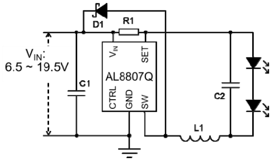
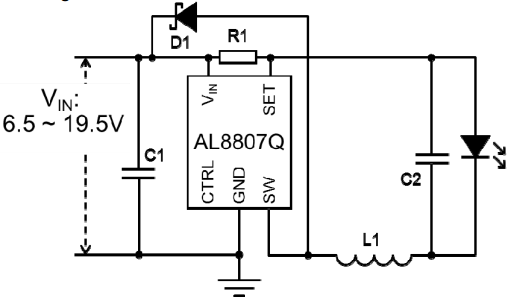
AL8807Q Typical Applications Circuit

AL8807Q Absolute Maximum Ratings (@TA= +25°C, unless otherwise specified.)
Symbol
| Parameter
| Ratings
| Unit
|
ESD HBM
| Human Body Model ESD Protection
| 4000
| V |
ESD MM
| Machine Model ESD Protection
| 300 | V
|
ESD CDM
| Charged Device Model ESD Protection
| 1000 | V
|
VIN | Continuous VIN pin voltage relative to GND | -0.3 to +40
| V
|
VSW
| SW voltage relative to GND
| -0.3 to +40
| V
|
VCTRL
| CTRL pin input voltage
| -0.3 to +6
| V
|
ISW-RMS | DC or RMS Switch current
| 1.6 | A |
ISW-PK | Peak Switch current (<10%)
| 2.5 | A |
TJ | Junction Temperature
| +150
| °C
|
TLEAD
| Lead Temperature Soldering
| +300
| °C
|
TST
| Storage Temperature Range
| -65 to +150
| °C
|
Caution: Stresses greater than the 'Absolute Maximum Ratings' specified above, may cause permanent damage to the device. These are stress ratings only;
functional operation of the devic e at these or any other conditions exceeding those indicated in this specification is not impl ied. Device reliability may be
affected by exposure to absolute maximum rating conditions for extended periods of time.
Semiconductor devices are ESD sensitive and may be damaged by ex posure to ESD events. Suitable ESD precautions should be taken when handling
and transporting these devices.
Recommended Operating Conditions (@TA= +25°C, unless otherwise specified.)
Symbol
| Parameter
| Min
| Max
| Unit
|
VIN
| Operating Input Voltage relative to GND
| 6.0
| 30
| V |
VCTRLH
| Voltage High for PWM dimming relative to GND
| 2.6
| 5.5 | V |
VCTRLDC
| Voltage range for 20% to 100% DC dimming relative to GND
| 0.5
| 2.5 | V |
VCTRLL
| Voltage Low for PWM dimming relative to GND
| 0
| 0.4 | V |
fSWV
| Maximum switching frequency
| —
| 1 | MHz
|
ISW
| Continuous switch current
| —
| 1.3 | A |
TJ | Junction Temperature Range
| -40
| 125 | °C
|
AL8807Q Application Information
The AL8807Q is a hysteretic (also known as equal ripple) LED driver with integrated power switch. It is available in two packages that provide a PCB area-power dissipation capability compromise. It is recommended t hat at higher LED currents/smaller PCBs that the MSOP-8EP version is used to maximize the allowable LED current over a wider ambient temperature range.
AL8807Q Operation
In normal operation, when voltage is applied at +VIN, the AL8807Q internal switch is turned on. Curr ent starts to flow through sense resistor R1,
inductor L1, and the LEDs. The current ramps up linearly, and the ramp rate is determined by the input voltage +Vin and the inductor L1.
This rising current produces a voltage ramp across R1. The internal circuit of the AL8807Q senses the voltage across R1 and applies a proportional voltage to the input of the internal comparator.
When this voltage reaches an internally set upper threshold, the internal switch is turned off. The inductor current continues to flow through R1, L1, the LEDs and the schottky diode D1, and back to the supply rail, but it decays, with the rate of decay determined by the forwar d voltage drop of the LEDs and the schottky diode.
This decaying current produces a falling voltage at R1, which is sensed by the AL8807Q. A volt age proportional to the sense voltage across R1 is applied at the input of the internal comparator. When this voltage falls to the internally set lower threshold, the internal sw itch is turned on again. This switch-on-and-off cycle conti nues to provide the average LED curr ent set by the sense resistor R1.
LED Current Control AL8807Q
The LED current is controlled by the resistor R1 in Figure 30.

Typical Application Circuit
Connected between VIN and SET the nominal average output current in the LED(s) is defined as:

For example for a desired LED current of 660mA and a default voltage VCTRL=2.5V the resulting resistor is:

AL8807Q Analog Dimming
Further control of the LED current can be achieved by driving the CTRL pin with an external voltage (between 0.4V and 2.5V); th e average LED current becomes:

With 0.5V ≤ VCTRL ≤ 2.5V the LED current varies linearly with VCTRL, as in figure 2. If the CTRL pin is brought higher than 2.5V, the LED current will
be clamped to approximately 100% and follows

When the CTRL voltage falls below the threshold, 0.4V, the output switch is turned off which allows PWM dimming.
AL8807Q PWM Dimming
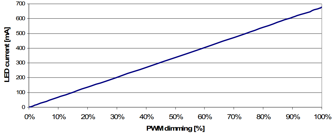
LED current can be adjusted digitally, by applying a low frequency Pu lse Width Modulated (PWM) logic signal to the CTRL pin to turn the device on and off. This will produce an average output current proportional to the duty cycle of the control signal. In particular, a P WM signal with a max resolution of 10bit can be applied to the CTRL pin to change the output current to a value below the nominal average value set by resistor RSET. To achieve this resolution the PWM frequency has to be lower than 500Hz, however higher dimming frequencies can be used, at the expense of dimming dynamic range and accuracy.
Typically, for a PWM frequency of 500Hz the accuracy is better than 1% for PWM ranging from 1% to 100%.

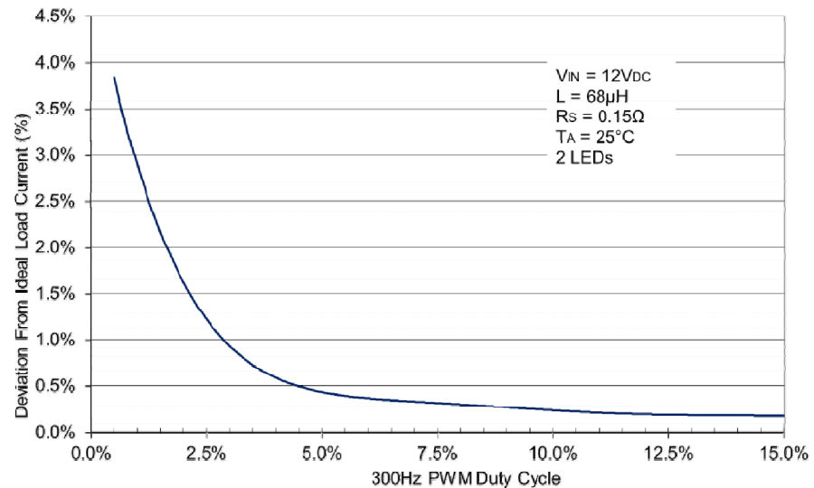
Zooming in at duty cycles below 10% shows:

The accuracy of the low duty cycle dimming is affected by both the PWM frequency and also the switching frequency of the AL8807Q. For best accuracy/resolution the switching frequency should be increased while the PWM frequency should be reduced.
The CTRL pin is designed to be driven by both 3.3V and 5V logic le vels directly from a logic out put with either an open drain o utput or push pull output stage.
AL8807Q EMI and Layout Considerations
The AL8807Q is a switching regulator with fast edges and measures small differential voltages; as a result of this care has to be taken with decoupling and layout of the PCB.To help with these effects the AL8807Q has been developed to minimise radiated emissions by co ntrolling the switching speeds of the internal power MOSFET. The rise and fall times are controlled to get the right compromise between powe r dissipation due to switching losses and radiated EMI. The turn-on edge (falling edge) dominates the radiated EMI which is due to an interaction between the Schottky diode (D1), Switching MOSFET and PCB tracks. After the Schottky diode reverse recovery time of around 5ns has occurre d; the falling edge of the SW pin sees a resonant loop between the Schottky diode capacitance and the track inductance, LTRACK, See figure 36.

PCB Loop Resonance
The tracks from the SW pin to the Anode of the Schottky diode, D1, and then from D1’s cathode to the decoupling capacitors C1 should be as short as possible. There is an inductance internally in the AL8807Q this can be assumed to be around 1nH. For PCB tracks a figure o f 0.5nH per mm can be used to estimate the primary resonant frequency. If the track is capable of handling 1A increasing the thickness will have a minor effect on the inductance and length will dominate the size of the induct ance. The resonant frequency of any oscillation is determined by the combined inductance in the track and the effect ive capacitance of the Schottky diode.
Recommendations for minimising radiated EMI and ot her transients and thermal considerations are:
1. The decoupling capacitor (C1) has to be placed as close as possible to the V IN pin and D1 Cathode
2. The freewheeling diode’s (D1) anode, the SW pin and the inductor have to be placed as close as possible to each other to avo id ringing.
3. The Ground return path from C1 must be a low impedance path with the ground plane as large as possible
4. The LED current sense resistor (R1) has to be placed as close as possible to the V INand SET pins.
5. The majority of the conducted heat from the AL8807Q is through the GND pin 2. A maximum earth plane with thermal vias into a second earth plane will minimise self-heating
6. To reduce emissions via long leads on the supply input and LEDs low RF impedance capacitors (C2 and C5) should be used at th e point the wires are joined to the PCB.


