


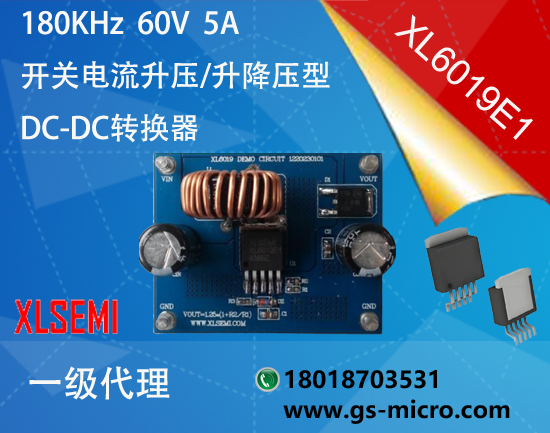
XLSEMI Primary Agent Boost-Buck DC-DC Regulator XL6019E1
- Model:
- XL6019E1
- Brand:
- XLSEMI
- Batch No:
- XL6019,XL6019E1, 升压 DC-DC 芯片,升降压电源 IC,5A 开关电源芯片,180KHz 升压芯片,TO263-5L, 广晟微 XL6019, 车载升压电源芯片,SEPIC 电源芯
- Desc:
- -
- Stock:
- 80000 只
XL6019E1 180KHz 60V 5A Boost-Buck DC-DC Converter | TO263-5L Wide Voltage Power IC
※ Note: XL6019E1 shares identical electrical specs with XL6012, only differs in package. TO263-5L features superior thermal dissipation, ideal for enclosed equipment running full load continuously, max output current reaches 2.1A.
Product Overview
XL6019E1 is a monolithic boost / boost-buck DC-DC switching IC developed by XLSEMI, belonging to XL60XX boost constant voltage series. Adopts current-mode PWM control with fixed 180KHz switching frequency, integrated 5A high-power internal MOSFET, supporting wide DC input from 5V to 40V.
A single FB pin embeds stable 1.25V voltage reference. By configuring external divider resistors, designers can set standard output voltages including 12V, 24V, 36V, 48V. It is compatible with three mainstream power topologies: Boost Step-up, SEPIC Boost-Buck, Inverting Dual Positive/Negative Power Supply.
Fully integrated protection circuits include soft-start, internal loop compensation, SW 60V overvoltage protection, cycle-by-cycle current limiting, thermal shutdown and input under-voltage lockout. Equipped with TTL-level EN enable pin for MCU low-power sleep control, fewer peripheral components lower PCB design barriers greatly.
Comes with TO263-5L package with large exposed thermal pad. Supplied in 800pcs tape & reel, compliant with RoHS & Halogen-free standards. Mass production solution for automotive DC power, industrial power supply, outdoor energy storage, LED driver, audio op-amp circuits and portable testing instruments.
XL60XX Boost Converter Series Selection Guide
| Model | Input Voltage | Switch Current | Switch Frequency | Output Range | Typical Output | Max Efficiency | Package | Rated Power |
|---|---|---|---|---|---|---|---|---|
| XL6007 | 3.6V-24V | 2A | 400KHz | 5V~60V | 24V/0.3A | 94% | SOP8 | ≤8W |
| XL6008 | 3.6V-32V | 3A | 400KHz | 5V~60V | 24V/0.7A | 94% | TO252-5L | ≤20W |
| XL6012 | 5.0V-40V | 5A | 180KHz | 8V~60V | 24V/1.3A | 95% | TO220-5L | ≤100W |
| XL6019E1 | 5.0V-40V | 5A | 180KHz | 8V~60V | 24V/1.2A | 94% | TO263-5L | ≤100W |
Selection Tips: XL6019E1 and XL6012 share identical electrical parameters, only package thermal design differs. TO263-5L with 30℃/W thermal resistance performs better for sealed enclosures operating full load continuously. XL6007 / XL6008 are cost-effective low-current options for low-power projects.
Core Product Advantages
5V to 40V ultra-wide input range, compatible with single/multi-cell lithium battery, 12V/24V vehicle battery, 24V industrial bus and 36V DC power supplies.
Stable internal 1.25V feedback reference. Matched with 1% precision metal film divider resistors to achieve accurate 12V / 24V / 36V / 48V output with tiny voltage error.
Built-in 5A peak current limit power MOSFET, SW pin withstand up to 60V, stable operation under high-power boost conditions, maximum full-load output current reaches 2.1A.
Fixed 180KHz low-frequency switching, integrated internal loop compensation without external RC network, low output ripple and easier EMC rectification.
Complete hardware protection set: soft-start to eliminate inrush current, SW 60V OVP, cycle-by-cycle OCP, thermal auto-shutdown, input UVLO protection.
TTL-level EN pin control: chip disabled below 0.8V, enabled above 1.4V, floating pin defaults to ON. Perfect for MCU sleep mode with only 70~100μA shutdown leakage current.
Peak conversion efficiency up to 94%, less heat generation at equivalent power, saves heat sink cost with outstanding line & load regulation performance.
TO263-5L package with large thermal exposed pad, thermal resistance 30℃/W without heat sink. Back metal pad connected to SW pin for enhanced PCB heat dissipation via copper area.
Single IC supports Boost / SEPIC / Inverting dual power topologies, reduces BOM stock varieties for multiple voltage output projects.
XL6019E1 Pinout Diagram (TO263-5L Package)
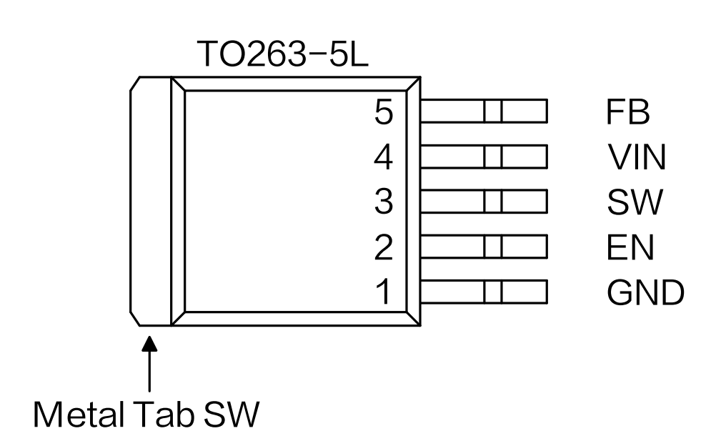
| Pin No. | Pin Name | Function Description |
|---|---|---|
| 1 | GND | Common power & signal ground, use large copper pour on PCB to reduce parasitic resistance |
| 2 | EN | Chip enable pin; shut down when V<0.8v,>1.4V, floating = default ON |
| 3 | SW | Power switching node connected to inductor & Schottky diode, internal 60V OVP, back pad shorted to SW |
| 4 | VIN | DC power input pin (5~40V), place electrolytic + MLCC close to pin for noise filtering |
| 5 | FB | Voltage feedback sampling pin with internal 1.25V reference. Route away from power loop, set output via R1/R2 divider |
Key Electrical Parameters (Ta=25℃ Standard Test)
| Parameter | Typical Value | Spec Range | Unit |
|---|---|---|---|
| Operating Input Voltage | 12 | 5~40 | V |
| FB Reference Voltage | 1.25 | 1.213~1.287 | V |
| Switching Frequency | 180 | 144~253 | KHz |
| Peak Switch Limit Current | 5 | Max 5 | A |
| SW Max Withstand Voltage | 60 | Max 60 | V |
| MOS On Resistance | 110 | 110~120 | mΩ |
| Max Duty Cycle | 90 | 0~90 Linear Adjustable | % |
| No-load Quiescent Current | 2.5 | 2.5~5 | mA |
| EN Shutdown Leakage | 70 | 70~100 | μA |
| Typical Efficiency | 93 | Up to 94+ | % |
Absolute Maximum Ratings (Exceeding Will Permanently Damage IC)
| Parameter | Limit Value | Unit |
|---|---|---|
| Input Voltage Range | -0.3~45 | V |
| SW Pin Max Voltage | -0.3~60 | V |
| Operating Junction Temp. | -40~125 | ℃ |
| Storage Temperature | -65~150 | ℃ |
| Thermal Resistance (No Heat Sink) | 30 | ℃/W |
| HBM ESD Rating | >2000 | V |
Output Voltage & Divider Resistor Calculation
Standard Output Formula: VOUT=1.25×(1+R2/R1). Recommended R1 value: 1KΩ ~ 10KΩ. Use 1% tolerance metal film resistors for high precision output.
Official Standard Resistor Matching Schemes:
1. Vin=12~22V, Vout=24V: R1=2.7KΩ, R2=49.9KΩ
2. Vin=5V, Vout=12V: R1=2.74KΩ, R2=24KΩ
3. Vin=10~32V, Vout=36V: R1=2KΩ, R2=56KΩ
4. Vin=20~40V, Vout=48V: R1=2KΩ, R2=75KΩ
5. SEPIC Vin=10~30V, Vout=12V: R1=2.74KΩ, R2=24KΩ
Design Suggestion: Keep duty cycle between 30%~70% for best efficiency & stability under large Vin-Vout difference. Max recommended output for 12V input: 40V; max output for 24V input: 56V.
Peripheral Component Selection Guide (XL60XX Official Design Manual)
1. Power Inductor Selection
Inductance Formula: L=(VIN×D×(1-D))÷(0.3×IOUTMAX×FSW), D=duty cycle, VD=Schottky forward voltage drop.
Selection Tips: Low DCR iron silicon alloy core inductor with saturation current ≥5A recommended (47uH/5A model). Iron silicon core gains 5% higher efficiency than iron powder core. Min input peak inductor current ~3.65A, sufficient saturation margin required.
2. Input Capacitor Selection
Rated voltage = 1.5 × Max input voltage, capacitance range 10~100uF. Combine electrolytic + 0.1~1uF MLCC placed close to VIN pin to suppress high-frequency noise. Capacitor RMS current ≥0.3 × inductor ripple current.
3. Freewheeling Diode Selection
Schottky diode mandatory, lower Vf for higher efficiency. Rated current ≥1.5 × max output, reverse voltage derated 30%. MBRD1045 for 24V designs; FSV10100 for 48V high-power circuits.
4. Output Capacitor Selection
Low ESR electrolytic preferred, voltage rating ≥1.5 × output voltage. Typical 220uF/35V for 24V/1A application to reduce output voltage ripple.
Standard Topology Schematic Diagrams
Basic Boost Step-up Circuit (12V Input to 24V Output Demo):
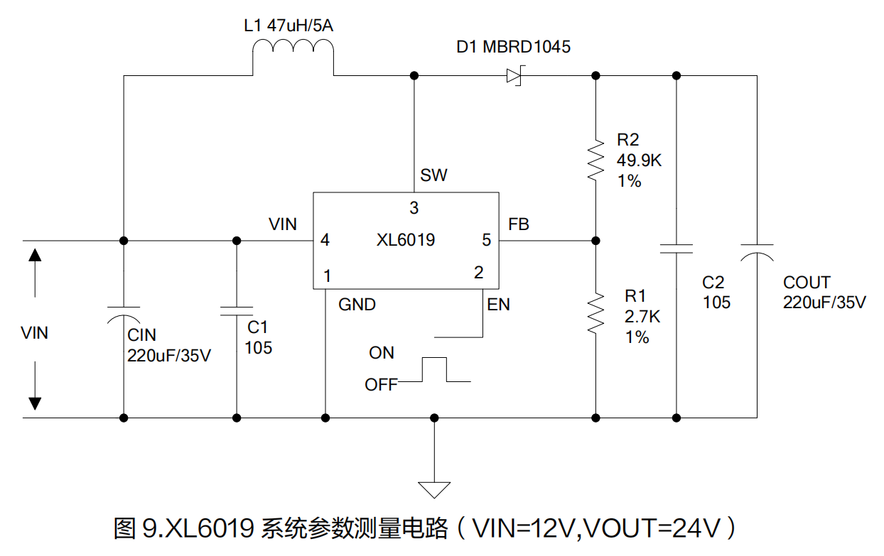
Suitable for automotive & industrial adapters, 47uH/5A inductor + MBRD1045 diode, 220uF input/output caps, stable 1.2A output current.
SEPIC Boost-Buck Circuit (Battery Variable Voltage System):
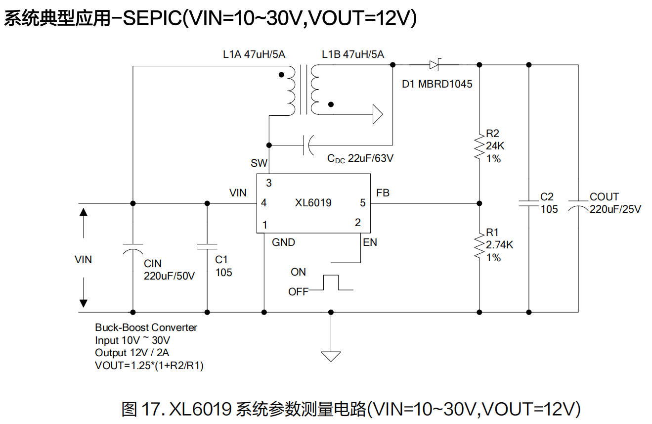
Stable regulation whether input higher or lower than output. Dual 47uH inductors + 22uF DC blocking cap, ideal for lithium battery & outdoor energy storage equipment with volatile voltage.
Inverting Dual ±12V Power Circuit (Audio Op-Amp Supply):
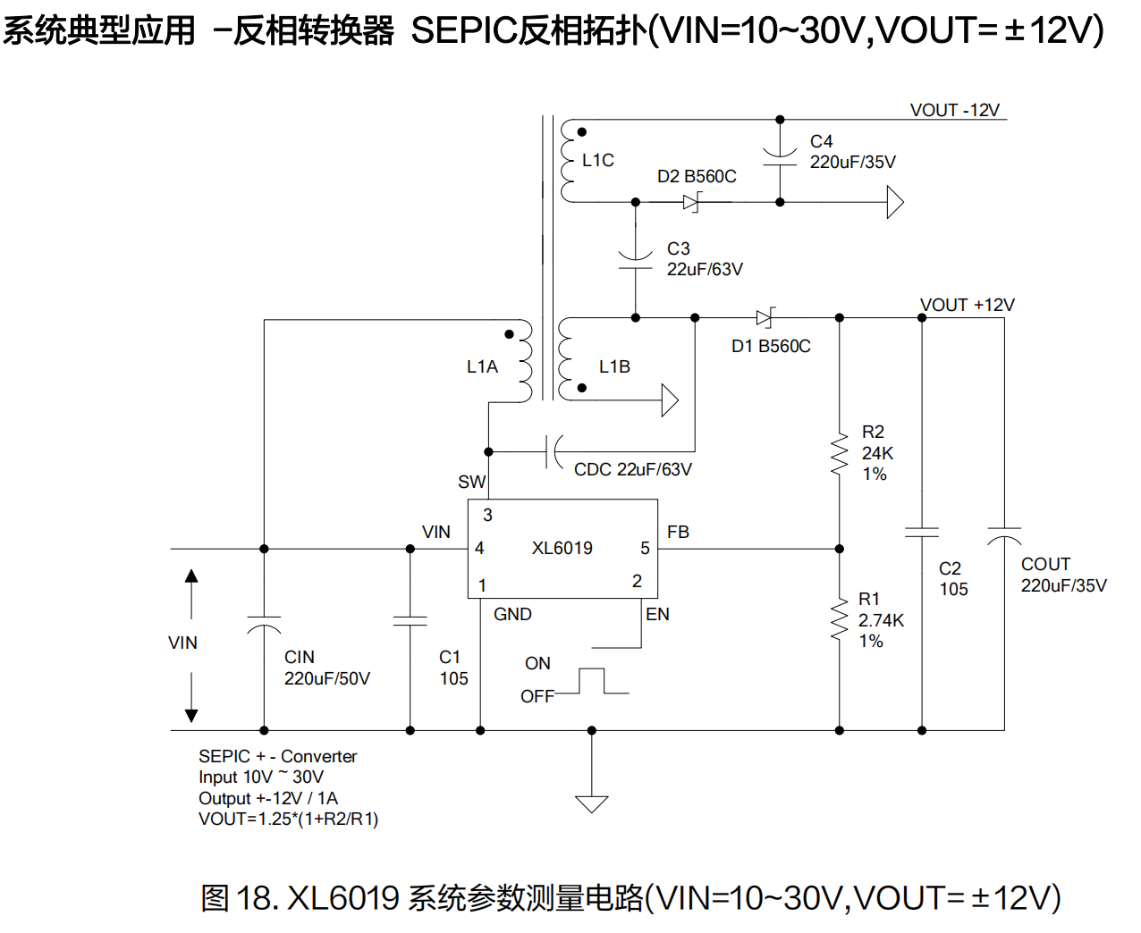
Single IC generates +12V & -12V simultaneously, eliminates extra power chip, low output ripple for audio amplifiers & operational amplifier circuits.
High Power Boost Circuit (36V to 48V Telecom Aux Power):
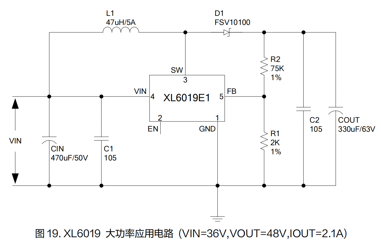
Upgrade input & output capacitance, adopt 100V FSV10100 fast recovery Schottky, steady 2.1A full load for industrial 48V communication power supply.
PCB Layout Design Tips
Widen tracks for VIN, GND, SW, VOUT high-current loops to cut parasitic impedance & temperature rise, reduce voltage ripple.
Place input electrolytic + MLCC capacitors as close as possible to VIN & GND pins to shorten high-frequency noise loop.
Route FB feedback trace far away from power inductor, Schottky & SW switching node. Use ground copper shielding to avoid switching noise causing output drift.
Spread large copper area under SW pad, power inductor & Schottky (major heat sources) for uniform heat dissipation and prevent local overheating.
Ordering Specifications
| Part Number | Marking Code | Package | Compliance Standard | Packaging |
|---|---|---|---|---|
| XL6019E1 | XL6019E1 | TO263-5L | RoHS & Halogen Free | 800pcs Tape & Reel |
Detailed Application Industries & Devices
| Industry Field | Target Equipment | Recommended Topology |
|---|---|---|
| Automotive Electronics | Vehicle EPC, Laptop Car Charger, On-board Camera, Truck LED Headlight, Autonomous Vehicle Lamp | Boost Circuit |
| Industrial Equipment | 24V to 48V Industrial PSU, Sensor High Voltage Power, Portable Tester, Telecom Aux Power | High-power Boost Circuit |
| Portable Handheld Devices | Battery Tester, Outdoor Energy Storage, Hand Torch, Mining Lamp, Plant Grow Light | SEPIC Boost-Buck Circuit |
| Security & Surveillance | IP Camera, Access Control Power, Outdoor Centralized Power, Infrared Device Supply | 12V to 24V / 36V Boost |
| Audio Analog Circuits | Audio Amplifier, Op-Amp Board, Audio Decoder, Mixer Dual Supply | Inverting SEPIC ±12V Power |
| LED Lighting | High-power Street Light, Industrial Floodlight, Wall Washer, Advertising Light Strip, Battery LED Lamp | Wide-Voltage Boost Circuit |
Automotive Application: 12V / 24V vehicle battery voltage fluctuates drastically. 5~40V wide input matches vehicle system perfectly, built-in multi-protection prevents spike voltage from damaging LED & surveillance hardware during engine startup.
Industrial Application: Convert factory 24V / 36V DC bus to standard 48V industrial rail. TO263 thermal package fits sealed control cabinets with low temperature under continuous full load.
Portable Battery Equipment: Lithium cell voltage varies 3V~4.2V. SEPIC topology maintains stable output whether input higher or lower than target voltage, eliminates multiple power designs.
Audio Circuit Application: Single IC generates dual positive/negative rail, cuts one power chip, simplifies PCB layout with ultra-low output ripple to eliminate audio background noise.
LED Driver Application: Built-in cycle-by-cycle current limit protects LED beads from overcurrent burnout, compatible with both battery and industrial DC input systems.
Common Failure & Troubleshooting FAQ
Q1: Chip destroyed after reverse input connection, how to solve?
Q2: SW pin broken by input voltage surge?
Q3: Actual output deviates from target voltage?
Q4: IC fails to boost after power-on?
Q5: Low overall power conversion efficiency?
Q6: Devices burnt under short-circuit output?
XL6007 (2A Low Power)
XL6008 (3A TO252 Package)
XL6012 (TO220 High Power Version)
Brand Authorization & Full Technical Support
GSMicro Semiconductor (Shenzhen) Co., Ltd. is authorized first-tier distributor of XLSEMI. Full stock of XL60XX series boost DC-DC converters, free sample service available for prototype & mass volume orders.
All purchases come with complete English datasheet, XL60XX full design handbook, multiple topology schematics & standard PCB layout reference. Our hardware team provides one-on-one technical consultation including divider calculation, component selection, EMC optimization & fault debugging for automotive, industrial, lighting certification projects.
- Grade And Comment
- Question And Answer